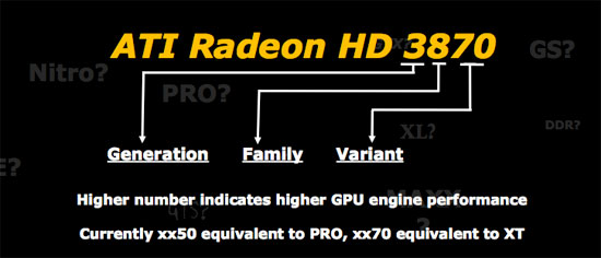
 A family mention, Radeon HD, followed by a four finger count. With the exception of the X2s, AMD has stuck to its name system without demerit. In fact, AMD has done such a dear job with keeping the names clean that things are the way they should be : the internal codenames are more unmanageable to remember than the actual names of the cards ( e.g. RV770 vs. Radeon HD 4870 ). NVIDIA however, merely has n’t gotten the touch. The GT200 plunge gave us two merely named cards : the GeForce GTX 280 and GTX 260, but it did n’t take long for NVIDIA to confuse the market with the launch of the GeForce 9800 GTX+. I hoped that the diagnose giddiness was limited to the older GeForce 9 GPUs, but nowadays it extended into the GTX batting order.
It ‘s called the GeForce GTX 260 Core 216. 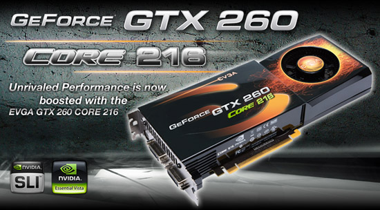
Holy terminology Batman The GeForce GTX 260 Core 216 ‘s name is actually quite descriptive, albeit absurdly long. The GeForce GTX 260 part we already know from the GT200 establish, the Core 216 suffix equitable indicates that the GPU has 216 “ cores ” ( besides playing on Intel ‘s modern Core i7 naming for Nehalem, ascribable away late this year ). Why NVIDIA did n’t just call it a GeForce GTX 265 or 270 is beyond me. To make matters worse, we ‘ll see companies adding their own suffixes to the already extended name. For example, EVGA sent us their core 216 called the EVGA GeForce GTX 260 Core 216 Superclocked Edition. possibly it ‘s some conspiracy to increase the wage of writers who get paid by the son. GTX 280 GTX 260 Core 216 GTX 260 9800 GTX+ 9800 GT Stream Processors 240 216 192 128 112 Texture Address / Filtering 80 / 80 72/72 64 / 64 64 / 64 56 / 56 ROPs 32 28 28 16 16 Core Clock 602MHz 576MHz 576MHz 738MHz 600MHz Shader Clock 1296MHz 1242MHz 1242MHz 1836MHz 1500MHz Memory Clock 1107MHz 999MHz 999MHz 1100MHz 900MHz Memory Bus Width 512-bit 448-bit 448-bit 256-bit 256-bit Frame Buffer 1GB 896MB 896MB 512MB 512MB Transistor Count 1.4B 1.4B 1.4B 754M 754M Manufacturing Process TSMC 65nm TSMC 65nm TSMC 65nm TSMC 55nm TSMC 55nm Price Point $420 – $500 $279 $250 – $300 $200 $130 – $170
If you remember the diagram below from our GT200 review you ‘ll see that a GeForce GTX 280 has ten clusters of 24 current processors ( the small blue blocks ), for a sum of 240 SPs or “ cores ”. The GeForce GTX 260 has eight of those clusters ( called Texture/Processor Clusters or TPCs ), bringing its sum up to 192 SPs. The core 216, as you can guess, has nine clusters or 216 SPs. NVIDIA equitable enabled another TPC on the Core 216 ( or alternatively, disabled a TPC on a GTX 280 ). 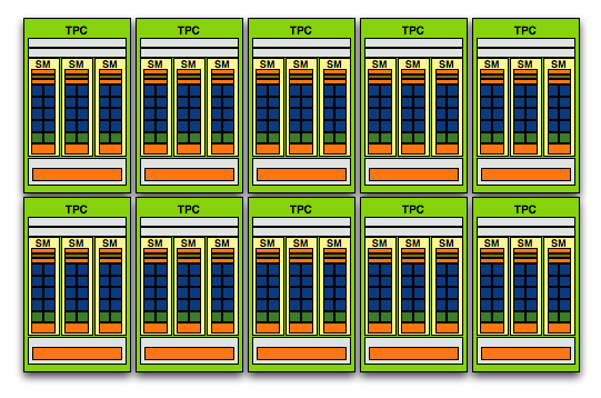
The GeForce GTX 280, 10 TPCs, 240 SPs 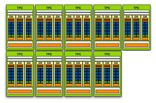
The GeForce GTX 260 Core 216, 9 TPCs, 216 SPs
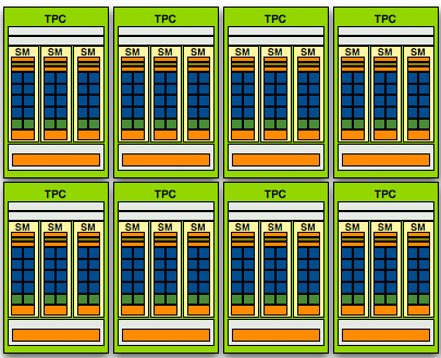
The GeForce GTX 260, 8 TPCs, 192 SPs The extra TPC besides gives the Core 216 another 8 texture address and filtering units, but the perch of the chip ‘s makeup remains the like, even devour to the clock speeds. The core 216 runs its core, shader and memory clocks at the same frequencies as the vanilla GTX 260. Priced at $ 279, the Core 216 is a direct rival to AMD ‘s Radeon HD 4870 – sell at a exchangeable monetary value. The GTX 260 will continue to exist although sell at a cheaper price charge and naturally with more process exponent, the GTX 280 remains unmoved .